
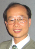
Prof. Liangchi Zhang, Southern University of Science and Technology
Fellow of the Australian Academy of Technological Science and Engineering
Liangchi Zhang is a chair professor at the Southern University of Science and Technology (SUSTech), Director of the Shenzhen Key Laboratory of Cross-scale Manufacturing Mechanics, and Director of the SUSTech Institute for Manufacturing Innovation. In 2006, he was elected to the Australian Academy of Technological Sciences and Engineering. Prior to SUSTech, Liangchi was a Scientia Professor at the University of New South Wales. He holds a BSc and MEng from Zhejiang University, a PhD from Peking University and a Higher Doctorate, Doctor of Engineering, from the University of Sydney. Liangchi has worked at Zhejiang University in China, Cambridge University in the UK, National Laboratory of Mechanical Engineering in Japan, University of Sydney and University of New South Wales in Australia. Liangchi’s research is in the area of advanced manufacturing, emphasizing both basic research and industrial applications. His work has led to significant technological and economic impacts. Liangchi is a highly cited scholar, has been granted many awards and honors globally, and is an author of seven monographs, more than 650 SCI journal papers, and an inventor of many new technologies.
Title:
Improving the shape accuracy of optical lenses by precision glass moulding
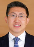
Prof. Yu Sun, University of Toronto
Fellow of the Canadian Academy of Engineering
Foreign Academician of the Chinese Academy of Engineering
Yu Sun is a Professor in the Department of Mechanical and Industrial Engineering, with joint appointments in the Institute of Biomaterials and Biomedical Engineering, the Department of Electrical and Computer Engineering, and the Department of Computer Science at the University of Toronto (UofT). He is a Tier I Canada Research Chair, and the founding Director of the UofT Robotics Institute. His Advanced Micro and Nanosystems Laboratory specializes in developing innovative technologies and instruments for manipulating and characterizing cells, molecules, and nanomaterials. He was elected Fellow of ASME (American Society of Mechanical Engineers), IEEE (Institute of Electrical and Electronics Engineers), AAAS (American Association for the Advancement of Science), NAI (US National Academy of Inventors), AIMBE (American Institute of Medical and Biological Engineering), CAE (Canadian Academy of Engineering), and RSC (Royal Society of Canada) for his work on micro-nano devices and robotic systems. He received a 2023 University of Toronto President’s Impact Award for his outstanding contributions to robotics at micro-nano scales, whose far-reaching impacts include transformative infertility treatments for patients and materials characterization techniques for industry.
Sun obtained his Ph.D. from the University of Minnesota in 2003 and did his postdoctoral research at ETH-Zürich. He joined the University of Toronto in 2004. In 2012-2013, he directed the University Nanofabrication Center as the faculty director. Sun has served and serves on the editorial boards of IEEE Trans. Robotics, IEEE Trans. Automation Science and Engineering, IEEE Trans. Mechatronics, J. Micromechanics Microengineering, Sensors and Actuators A: Physical, Scientific Reports, and Microsystems & Nanoengineering. Among the awards he received were the McLean Award in 2009; the IEEE Robotics and Automation Society Early Academic Career Award in 2010; eight times University of Toronto Connaught Innovation Award; two times First Prize for technical achievement of ASRM (American Society for Reproductive Medicine); an NSERC E.W.R. Steacie Memorial Fellowship in 2013; the IEEE C.C. Gotlieb Computer Award in 2018; the CSME Mechatronics Medal in 2020; an NSERC Synergy Award for Innovation in 2021; and over a dozen best paper awards and finalists in journals and at international conferences.
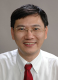
Prof. Minghui Hong, Xiamen University
Fellow of the Singapore Academy of Engineering
Prof. Hong Minghui is the Tan Kah Kee Chair Professor, Xiamen University, Fujian, China. He is also the Engineering Technology Division Chairman and Dean of Pen-Tung Sah Institute of Micro-Nano Science and Technology of Xiamen University. Prof. Hong specializes in laser microprocessing & nanofabrication. He has co-authored 15 book chapters, 42 patents granted, and ~ 600 scientific papers and 100+ plenary/keynote/invited talks in international conferences. He is a member of organizing committees for Laser Precision Micromachining International Conference (2001~2024), International Symposium of Functional Materials (2005, 2007 and 2014), Chair of International Workshop of Plasmonics and Applications in Nanotechnologies (2006), Chair of Conference on Laser Ablation (2009) and Chair of Asia-Pacific Near-field Optics Conference (2013 and 2019). Prof. Hong is invited to serve as an Editor ofLight: Science and Applications, Engineering, Science China G,Laser Micro/nanoengineering, and Executive Editor-in-chief ofOpto-Electronic Advances and Opto-Electronic Science. Prof. Hong is Fellow ofAcademy of Engineering, Singapore (FSEng), Fellow of Optical Society of America (OPTICA), Fellow ofInternational Society for Optics and Photonics (SPIE),Fellow of International Academy of Photonics and Laser Engineering (IAPLE)and Fellow of Institution of Engineers, Singapore (IES).As an active tech entrepreneur, he is also the leading founder ofPhaos Technology Pte. Ltd., Opto Science Pte. Ltd. and Xiamen Light Technology Integration Pte. Ltd.
Title:
Engineered Microsphere and Compound Lens for Optical Nano-Imaging
Abstract:
Microsphere nanoscope as a competitive nano-imaging technique has extensive applications in the semiconductor industry and biology due to its real-time imaging ability, label-free characteristics, and good compatibility with conventional microscopes. After years of rapid development, microsphere nanoscope still faces restrictions on imaging resolution, contrast, magnification, and field-of-view. To further promote the imaging performance of microsphere nanoscope, two new technical modification routes are developed. At single component level, engineered microspheres with enhanced nano-imaging ability, such as hyper-hemi-microsphere and bilayer-film-decorated microsphere, are put forward and realized through diverse nanofabrication techniques. At device level, substituting single microsphere with microsphere compound lens can improve imaging performance in multiple aspects, such as customized magnification and large field-of-view. Effectiveness of these modifications has been proved in semiconductor chip inspection and microfluidic dynamic nano-imaging. Furthermore, these technical advances pave way for a miniaturized all-microspheres nanoscope with an ultra-compact system configuration, which makes low-cost and portable nanoscopes feasible.

Prof. Shulian Zhang, Tsinghua University
Shulian Zhang, male, professor, laser nano-measurement expert, Fellow of the Chinese Society of Instrumentation, Fellow of the Optical Society of America, Fellow of the Chinese Optical Society,founder of orthogonal polarization laser nano-measurement technology in China and one of the main international founders. As the first accomplisher, he has won two of second prizes of National Technical Invention (2007 and 2010), two of first prizes of natural Science of Ministry of Education, and one of first prize of Invention of Electronic Society. He was awarded the Lifetime Contribution Award at ISMTII-2017 International conference. As the first author, he has published four monographs, edited two collections of international conferences and one issue of “The professor talks about precision measurement” for Journal of Measurement Technology. He has published more than 360 papers and more than 80 invention patents. As the head of The Chinese side, he organized 5 academic bilateral meeting between China/Germany and China/Britain.
Title:
Metrology Applications of Orthogonally Polarized Lasers
Abstract:
The laser orthogonal polarization phenomena and the applications of these phenomena as the principles of nanoscale measuring instruments. The instruments include: birefringent dual-frequency laser and interferometer, laser frequency split optical phase delay/internal stress measuring instruments, laser nano-measurement ruler, laser-feedback on-line optical phase retardation measuring instruments, micro-chip laser common path frequency-shift feedback interferometers etc.. The report will also describe the application status of these instruments.

Wei Gao, Tohoku University
Fellow of Engineering Academy of Japan
Wei Gao received his Bachelor from Shanghai Jiao Tong University in 1986, followed by MSc and Ph. D from Tohoku University in 1991 and 1994, respectively. He is currently a professor in Tohoku University. His research interests lie primarily in precision nanometrology. He is an author of the books “Precision Nanometrology” (Springer), “Surface Metrology for Micro- and Nanofabrication” (Elsevier), “Optical Metrology for Precision Engineering” (De Gruyter). He was awarded the Prize for Science and Technology from the Ministry of Education, Culture, Sports, Science and Technology (MEXT), Japan, in 2019. He is a fellow of CIRP, ISNM, JSPE and a Fellow of The Engineering Academy of Japan (EAJ).
Title:
Advances in optical dimensional metrology for precision engineering
Abstract:
Precision engineering is a discipline to develop and apply principles of design, manufacture, control and measurement for precision machines and precision manufacturing. Precision dimensional metrology is one of the cornerstones to support precision engineering. Among the various types of measurement methods, optical methods with noncontact, fast, and sensitive features are playing an increasingly important role in precision dimensional metrology where accurate measurements are required to be made in a short time and with minimal influence on the measurement target, i.e., machines and parts. In the first part of this speech, advances in commercially available measuring instruments of optical dimensional metrology, such as laser interferometer, optical encoders, autocollimators, optical microscopes are presented. In the second half, state-of-the-art research activities on optical dimensional metrology, such as multi-axis optical encoders/ autocollimators, as well as the next-generation optical metrology systems based on ultrashort pulse laser and optical frequency comb will then be demonstrated.

Prof. Yossi Rosenwaks, Tel-Aviv University
Chair Professor Nanoelectronics, former Dean of Engineering. Yossi is a Professor of Electrical Engineering at TAU since 2005 after joining the faculty in 1996, and currently a member of Israel higher council of education (CHE), and managing director of Fraunhofer Innovation Platform (FIP) for sensors. Prof. Rosenwaks current research interests include nanowire transistors and sensors, two-dimensional materials and devices, and charge carrier dynamics and transport in semiconductors. Prof. Rosenwaks is a co-author of more than 200 peer reviewed articles, 10 international patents, has presented 75 invited talks at international meetings, and has supervised more than 70 PhD and MSc students, 8 of which are currently faculty at top research universities. He served as the president of the Israel Vacuum Society (2003-2006), and as the director of TAU’s Wolfson Center for Applied Materials Research and Gordon Center for Energy Studies (2005-2008), and the head of the Physical Electronics department (2011-14), and the Dean of the Faculty of Engineering (2014-2022).
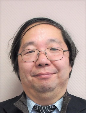
Prof. Ken-ya Hashimoto, University of Electronic Science and Technology of China
He joined Chiba University, Chiba, Japan, as a Research Associate in 1980 and retired there as a Professor Emeritus in 2021. Right after retirement, he moved to the University of Electronic Science and Technology of China, Chengdu, China, as a Professor. He received the Dr. Eng. degree from the Tokyo Institute of Technology, Tokyo, Japan, in 1989.
He received IEEE Fellow (2005), International Distinguished Lecturer Award (2005) and Distinguished Service Award (2019) both from the IEEE UFFC Society, Ichimura Industrial Award from the New Technology Development Foundation (2015), and The Commendation for Science and Technology by the Minister of Education, Culture, Sports, Science and Technology for Research (2018).
His current research interests include simulation and design of various high-performance surface and bulk acoustic wave devices.
Title:
Optical Diagnosis of RF SAW/BAW Devices in Multi-GHz Range
Abstract:
Optical sensing of acoustic vibrationis well recognized as a versatile diagnosis tool for surface and bulk acoustic wave (SAW/BAW) devices, which are widely used in the radio frequency (RF) front-end of smart phones. Information captured by optical sensing may offer betterunderstanding of their operation state, which often results in further enhancement of device performances.
The author and his coworkers started to develop a fast-mechanical scanning and phase-sensitive laser probe system for RF SAW/BAW devices in 2003.The system has been evolved sustainably for more than 20 years to fulfill requests given by these outside users.Various unique functions were developed and their implementation made the system more useful and easier to use also for users.
This paper details the optical probing system developed by the author’s group. In addition to the optical setup, employed detection electronics, mechanical scan scheme and various supporting techniques are detailed. Some measured data are given and their use for the device diagnosis is demonstrated.
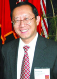
Prof. Zhouling Wu,ZC Optoelectronic Technologies. LTD.

Prof. Gaoliang Dai, Physikalisch -Technische Bundesanstalt
Title:
Accurate and traceable nanoscale dimensional metrology
Abstract:
Nanometrology covers a wide range of metrology techniques for enabling characterisation and measurement of nanomaterials, structures, components, devices, and systems at the nanoscale. Adequate nanometrology is key to innovations in nanotechnology and nanoscience, such as understanding the interaction mechanism between atoms, controlling nanomanufacturing processes, optimising nanoscale products as well as preventing nanotoxicity. Nanometrology is closely related to industry sectors such as semiconductor, automotive, nanomaterial and nanophotonics, and has major economic, environmental, and social impacts on our economy and daily lives.
This keynote paper will offer an overview of recent advancements for accurate and traceable nanoscale dimensional metrology, particularly using the atomic force microscopic (AFM) techniques. Two kinds of fundamental calibration tasks of nanometrology: (i) calibration of geometrical parameters (i.e. magnification, nonlinearity, orthogonality, etc.) and (ii) calibration of beam/tip geometry, will be focused.
To address above mentioned metrology challenges, some developments at the Physikalisch-Technische Bundesanstalt, the national metrology institute of Germany, will be introduced. One is the development of a unique high-speed large-range metrological AFM (HS LR-AFM), which has a capable measurement volume of 25 mm x 25 mm x 5 (x, y, z) and a measurement speed up to 1 mm/s. The HS LR-AFM is currently one of the key workhorses for satisfying versatile nanoscale calibration tasks with e.g. an expanded measurement uncertainty of 0.3 nm (k=2) for step height calibrations, and <10 pm (k=2) for mean pitch calibration of lateral standards. The other concerns the development of a new bottom-up traceability approach for true 3D nanometrology, where the three-dimensional geometries of complex nanostructures are ultimately calibrated to the lattice constant of crystal silicon. Excellent results have been achieved using this new traceability approach as well. For instance, together with a set of well-developed data evaluation algorithms and software, the AFM tip geometry can be calibrated with a measurement repeatability down to approx. 0.3 nm and an uncertainty down to approx. 1 nm. The critical dimension of line width standard can be calibrated with an expanded measurement uncertainty of 2.5 nm (k=2) or even below, as confirmed by international comparisons.
Some selected application examples of the developed nanometrology techniques will be presented: (i) development of an extreme ultraviolet (EUV) photomask standard; (ii) calibration of various nanoscale standards; and (iii) development of a novel material measure for characterising 2D Instrument Transfer Function (ITF) of various optical areal surface topography measurement tools.